The silicon brains running some of the world’s newest mobile phones and personal computers were made possible in part by advanced laser and plasma physics research at Lawrence Livermore National Laboratory (LLNL).
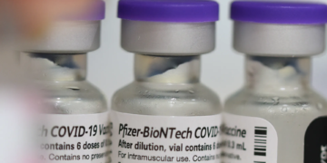
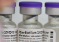
Last year, Apple’s iPhone 12s became the first mobile phones on the market powered by 5-nanometer (nm) microprocessors, which are manufactured using a transistor-packing extreme ultraviolet (EUV) lithography process that can be traced to work done by LLNL, Sandia National Laboratories and Lawrence Berkeley National Laboratory dating back to the 1990s.

In this 2008 photo, Lab materials scientist Paul Mirkarimi (left) and mechanical technician Jeff Robinson load a mask blank substrate for defect smoothing. Using the technique of defect smoothing, researchers planarize tiny particles and pits to render a nearly perfect surface for masks used in extreme ultraviolet lithography, a process developed to produce computer chips that are faster and have more memory. Credit: Jacqueline McBride.
The process, which uses EUV light to etch features that are as small as a few nanometers into chips and processors, is igniting a revolution sweeping through the semiconductor industry. Samsung last month unveiled a version of its flagship Galaxy S21 smartphone that will run on the company’s own EUV 5-nm chip, the Exynos 2100, although for now that version will be available only outside the North American and South Korean markets.
The production of smaller, more powerful and more efficient chips also should help the Lab in the near future.
“It’s great that we can buy a mobile phone that has a little bit of Livermore history encapsulated inside,” said physicist Craig Siders, commercial technology development leader for the National Ignition Facility & Photon Science Directorate (NIF&PS). “But the big payoff will be in a few years when we’ll be able to do our central Lab mission with computers that just absolutely could not have existed without this sort of technology.”
Industry partnerships
In 2016, the Lab entered into a cooperative research and development agreement (CRADA) about EUV lithography with ASML Holding NV, the Dutch-based firm that is the leading supplier of fabrication equipment to the world’s semiconductor industry.
ASML’s customers include silicon foundry giant Taiwan Semiconductor Manufacturing Co. (TSMC), which makes Apple’s A14 chip for the iPhone 12 lineup that began to roll out in October 2020 and the M1 chip for the newest model MacBook Pro, MacBook Air and Mac Mini computers introduced in November 2020. Samsung and Intel also are among ASML’s top customers.

This 2010 photo shows mirrors used in NASA’s Extreme Ultraviolet Imaging Telescope that imaged the solar atmosphere at several wavelengths. A Lab team used technology developed by the EUVL project to design and fabricate the reflective multilayer coatings. Credit: NASA.
The iPhone 12s are the first production mobile phones to use an EUV source to create chips with 5-nm features. This new technology allows the chip to be packed with about 11.8 billion transistors each about 25 atoms across. Industry reports say other semiconductor companies already are working on 4-nm processes and beyond.
Members of the teams that worked on EUV over the years were heartened to see EUV technology commercially available on mainstream consumer products.
“It’s a good example of the technology and capabilities developed at Livermore,” said computational physicist Steve Langer, “and in the case of that first CRADA, the other national labs, and how we were able to do some research to kickstart a project that in the end has a major commercial impact.
“It’s important to note that the early work did have an impact,” he added. “It really was foundational for what’s happening now in production fabrication plants.”
Pursuing Moore’s Law
In a nutshell, EUV lithography (EUVL) uses pulses of high-intensity carbon dioxide (CO2) lasers to heat tin droplets to temperatures at which they emit strong 13.5-nm EUV light. The EUV light allows vendors to pack more transistors onto a silicon wafer chip than is possible with the standard 193-nm sources used currently. The increased number of transistors allows Apple and other companies to put more computing power into their electronic devices.
The number of transistors in a chip increased in a steady cadence described by the well-known Moore’s Law. This “law” is actually an observation made in 1965 by Intel co-founder Gordon Moore, who noted that the number of transistors on a chip was doubling every 18 to 24 months.
For several generations, the wavelength of the light used in chip fabrication decreased as transistor size decreased. The industry looked to new technologies when it became apparent that traditional lasers operating at wavelengths shorter than 193 nm were not a viable option for the future. EUVL was one technology that long promised to push beyond those limitations by using a far shorter light wavelength of 13.5 nm. EUVL enables the cost-effective manufacture of smaller transistors.
Livermore’s laser legacy
EUVL development traces back to LLNL’s distinguished legacy of laser development and research that predates NIF, the world’s largest and highest-energy laser.
“The Lab has a very long history in the EUV community and with generations of this technology going back decades,” Siders said.
“Livermore had been shining lasers on solid disc targets since the early days,” Langer added.
The technology also became useful for other purposes. In February 2010, NASA launched its sun-imaging Solar Dynamics Observatory, a spacecraft that included mirrors with multilayer reflective coatings fabricated with technology LLNL developed as part of its research into EUV sources.
The chip industry, however, encountered roadblocks before it could turn EUV technology into a commercially viable option — particularly in finding ways to create powerful-enough high-repetition rate lasers and develop reliable, efficient manufacturing techniques to lower production costs enough to compete with existing technology.
“They didn’t have power anywhere near enough to do what industry needed,” Langer said. “Up to the 2016 time period, it was not clear they would actually be able to come up with a source with the required brightness. Pundits were saying it will never happen.”
EUVL and NIF
Meanwhile, NIF researchers continued with the facility’s own missions, including supporting NNSA’s Stockpile Stewardship Program to maintain the reliability and safety of the U.S. nuclear deterrent without full-scale testing and to make important advances toward achieving ignition in inertial confinement fusion (ICF) experiments in the laboratory for the first time.
These cutting-edge experiments rely on designs developed using supercomputers running complex multi-physics simulation codes. HYDRA is widely used to simulate ICF experiments and includes hydrodynamics, neutronics, magnetic fields and other processes that occur during an experiment on NIF.
It turns out that HYDRA could also be used for EUV simulations. “The number of dimensions to looking at how one of these tin targets are working is daunting and you really have to tackle it with one of these supercomputer codes,” Siders said.
With the 2016 CRADA, ASML researchers engaged with LLNL’s High Performance Computing Innovation Center and the NIF&PS Advanced Photon Technologies Program to help improve the performance of EUVL. That CRADA expired in August 2017, but ASML has gone on to produce systems that fueled the semiconductor industry’s push to release 7-nm mobile phone chips in 2019 and 5-nm chips just last year.
“It’s cool to see the industry get back to the Moore’s Law levels we had a few years ago,” Langer said.
LLNL researchers also plugged into the Lab’s expertise in ensemble supercomputer simulations, which take in a wide variety of parameters, to further explore EUVL.
“This was the first ensemble simulation of EUVL sources that anyone’s ever done,” Langer said. “So it’s neat that we can take Lab technology developed for one purpose and apply it to another.”
And while the pursuit of laser-driven ignition and creating silicon wafers with EUV light might “look like very disparate things,” Siders said, “the scale of the laser challenge is actually very similar. That’s why the national labs are here, to do these kinds of things.”
The chip industry will likely continue to ask more questions about EUV.
“Can EUVL sources operate at shorter wavelengths and still deliver high average power? Achieving that would be a big step toward continuing Moore’s Law increases in transistors per chip,” Langer said. “I think Livermore will have a lot to say in these areas.”
Source: LLNL


:quality(70)/cloudfront-eu-central-1.images.arcpublishing.com/irishtimes/CGYPT6WE7VAO3KJ773SHUVMVBY.jpg?resize=1200,630&ssl=1)