Scientists from the Korea Institute of Machinery & Materials (KIMM, President Sang Jin Park) under the Ministry of Science and ICT, and the Nanyang Technological University, Singapore (NTU Singapore, President Subra Suresh) have developed a technique to create a highly uniform and scalable semiconductor wafer, paving the way to higher cup yield, more cost-efficient semiconductors and mitigating the global chip shortage.
Semiconductor chips commonly found in smart phones and computers are difficult and complex to make, requiring highly advanced machines and special environments to manufacture. Their fabrication is typically done on silicon wafers and then diced into the small chips that are used in devices. However, the process is imperfect and not all chips from the same wafer work or operate as desired. These defective chips are discarded, lowering semiconductor yield while increasing production cost.
The ability to produce uniform wafers at the desired thickness is the most important factor in ensuring that every chip fabricated on the same wafer performs correctly.
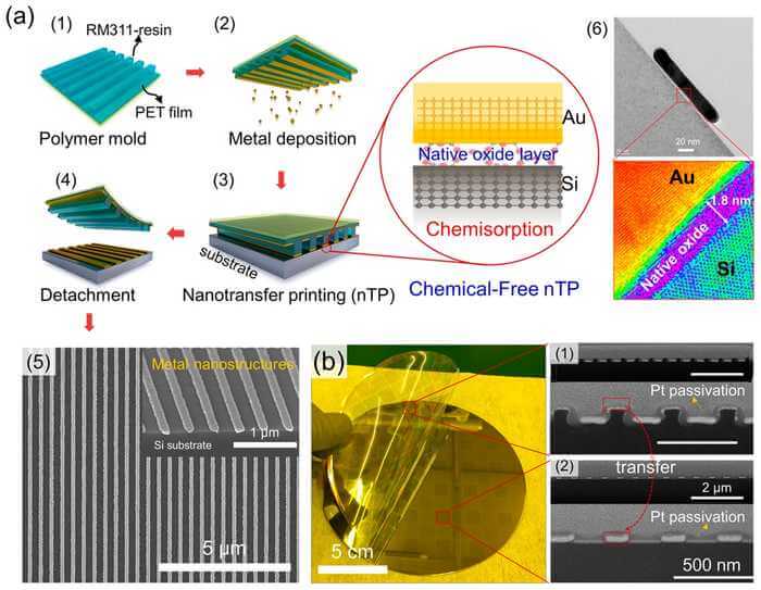
Nanotransfer-based printing – a process that uses a polymer mould to print metal onto a substrate through pressure, or ‘stamping’ – has gained traction in recent years as a promising technology for its simplicity, relative cost-effectiveness, and high throughput. However, the technique uses a chemical adhesive layer, which causes negative effects, such as surface defects and performance degradation when printed at scale, as well as human health hazards. For these reasons, mass adoption of the technology and consequent chip application in devices has been limited.
In their study, which was published in the peer-reviewed journal ACS Nanothe research team from KIMM and NTU reported that their chemical-free printing technique, when combined with metal-assisted chemical etching – a method used to enhance the contrast on surfaces to make nanostructures visible – resulted in semiconductor wafers with nanowires (nanostructures in cylindrical form) that were highly uniform and scalable. The semiconductor also demonstrated better performance when compared with current chips in the market. Moreover, the fabrication method is also fast and leads to high chip yield.
New chemical-free printing technique leads to high chip yield
The newly nanotransfer printing technique developed by KIMM and NTU is accomplished by transferring Gold (Au) nanostructure layers onto a Silicon (Si) substrate at low temperature (160 °C) to form a highly uniform wafer with nanowires that can be controlled to the desired thickness during fabrication.
The printing technique, which is chemical-free, works by triggering direct chemisorption of the thin metal films under heat – a chemical reaction that creates a strong bond between a substrate surface and the substance that is adsorbed.
This industrial compatible technique allows a wafer to be fabricated quickly and uniformly at scale (from nanometers to inches). At the same time, the fabricated wafer is almost defect-free, meaning that little to no chip are discarded due to poor performance. In lab tests, the joint research team was able to achieve more than 99 per cent yield transfer of a 20-nanometre thick Au film onto a six-inch Si wafer. This printable wafer size was limited to the laboratory setup, and the KIMM-NTU team believes their technique can easily be scaled up for use on a twelve-inch wafer – the mainstream wafer size in the current production lines of semiconductor chipmakers like Samsung, Intel and GlobalFoundries.
When the method was adopted to fabricate a six-inch wafer, results showed the printed layer remained intact with minimal bending during etching – a process that commonly cause layers to separate – demonstrating the outstanding uniformity and stability of the technique developed by KIMM and NTU.
Furthermore, when 100 light sensors, known as photodetectors, were fabricated into the six-inch wafer, excellent uniformity of performance was achieved, underlining its excellent potential for the technique to be used in commercial mass production.
Technique opens door to lower cost semiconductor chip
KIMM’s co-lead researcher Dr. Jun-Ho Jeong, Principal Researcher from the Nano-Convergence Manufacturing Systems Research Division (also the Director of Research Planning and Coordination Division), stated that “the technique developed by the KIMM-NTU team is a new concept of low-cost mass production technology for nanostructure, which can be applied to the mass production of nanophotonics, high performance nano-solar cells, next-generation secondary batteries and others.”
NTU’s co-lead researcher, Assistant Professor Munho Kim from the School of Electrical and Electronic Engineering, also added that the uniformity, scalability and stability of the team’s technique overcomes the main bottleneck present in existing nanotransfer printing methods, and it could also lead to significant advances in various electronics and light-based devices, as semiconductor chips may now be manufactured in a more cost-effective manner.
“The technique devised by the research team from KIMM and NTU has proven to be effective in creating wafer with excellent uniformity, which translates into fewer defective semiconductor chips. The reality of global chip supply is its vulnerability to many external factors, including shortage of materials and unexpected events like the supply chain disruptions caused by the COVID-19 pandemic. Our newly developed method thus has great potential to relieve the tension on the global chip supply in future by increasing chip yield. Moreover, chip makers may also enjoy greater cost-efficiency with higher yields,” said Asst. Prof. Kim.
Highlighting the significance of the work, Dr. Jeong further added that the collaboration between KIMM and NTU is an example of a successful international partnership which has led to the joint application of patents. The research team has filed for patents in Korea and Singapore for the technique they developed. The team spent three years to design, fabricate and test the new technique, which was carried out at NTU’s Nanyang NanoFabrication Centre (N2FC). As next steps, the research team is aiming to scale up their technique with an industrial partner for commercialization within the next few years.